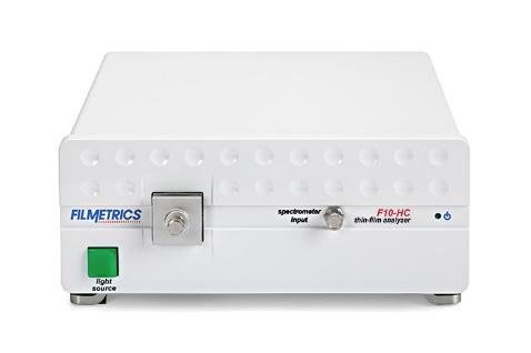
The Most Powerful Instruments Available for Monitoring Thin-Film Deposition


Measure deposition rates, film thickness, optical constants (n and k), and uniformity of semiconductors and dielectric layers in real-time with the F30 spectral reflectance system.
Example Layers
MBE and MOCVD: Smooth and translucent, or lightly absorbing films, may be measured with the F30 thickness measurement series instruments. This includes virtually any semiconducting material, from AIGaN to GaInAsP.
Model Specifications:
| Model | Thickness Range | Wavelength Range |
| F30 | 15nm – 70µm | 380-1050nm |
| F30-UV | 3nm – 40µm | 190-1100nm |
| F30-NIR | 100nm – 250µm | 950-1700nm |
| F30-EXR | 15nm – 250µm | 380-1700nm |
| F30-UVX | 3nm – 250µm | 190-1700nm |
| F30-XT | .2µm – 450µm | 1440-1690nm |
* Film stack dependent
Benefits:
- Dramatically improves productivity
- Low cost – Can pay for itself in months
- Accurate – Measure to better than ±1%
- Fast-Measurements in seconds
- Non-Invasive – Totally outside of deposition chamber
- Easy to use – Intuitive Windows® software
- Turn-key system sets up in minutes
Common Optional Accessories:
- NIST-Traceable Thickness Standard
- Lens Assemblies


Reviews
Clear filtersThere are no reviews yet.